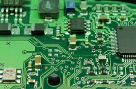
Determining the optimal number of PCB layers is crucial for designers aiming to balance performance, cost, and manufacturability of printed circuit boards (PCBs). This guide provides a detailed look at what influences this decision and how to select the right layer count for various applications.
What Determines the Number of Layers in a PCB?
The complexity of electronic devices varies dramatically, and so does the design of their PCBs. Several factors guide the decision on the number of layers:
Circuit Complexity and Component Density
Devices with higher component densities require more layers. A basic calculator might get away with a two-layer PCB, but a smartphone could need up to 10 layers. More layers provide the necessary space for traces and pads, reducing cross-talk and interference among components.
Signal Integrity
In high-speed applications, maintaining signal integrity is paramount. More layers allow for dedicated ground and power planes, which shield signal layers. For instance, an eight-layer PCB might feature two ground layers, two power layers, and four signal layers, enhancing the performance and reliability of the device.
Thermal Management
Electronic components generate heat, which needs to be managed effectively to maintain function and reliability. Additional layers can facilitate better heat distribution, especially when thermal vias are used to connect heat-generating components to a heat sink layer.
Ideal Layer Counts for Different Applications
When it comes to PCB design, more layers often mean better performance but also higher costs. Here’s a practical breakdown:
- Two to Four Layers: Ideal for simple consumer electronics and low-speed applications. These are cost-effective and sufficient for straightforward designs.
- Four to Six Layers: Common in more complex consumer devices and automotive applications where additional layers are used for power distribution and signal integrity.
- Eight Layers and Above: Necessary for high-performance products such as computer motherboards, telecommunications equipment, and advanced industrial machines. These layers accommodate multiple ground and power planes, crucial for minimizing electromagnetic interference (EMI).
Cost vs. Performance
The cost of manufacturing PCBs increases with each additional layer due to more materials and more complex fabrication processes. Designers must consider if the incremental cost of adding layers is justified by the improvement in performance and durability. For example, upgrading from a four-layer to a six-layer PCB might increase the cost by approximately 20%, but it could enhance signal integrity and reduce EMI by over 30%.
Real-world Application: A telecom company improved its network router’s performance by upgrading from a six-layer to a ten-layer PCB. This modification allowed for dedicated layers for high-speed data transmission, reducing latency and packet loss significantly.
Making the Decision
Choosing the right number of pcb layers depends on a nuanced understanding of the device’s requirements and the trade-offs involved. Designers must assess the need for additional layers against the backdrop of budget constraints and performance targets. This decision is not just technical but strategic, impacting the overall success of the product in its market.
In summary, while the ideal number of PCB layers varies, understanding the key factors—circuit complexity, signal integrity, and thermal management—allows for a tailored approach that aligns with both technological needs and business objectives.

